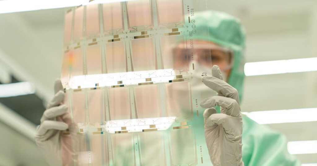
ASML and TSMC have formed a collaborative industry initiative to move High NA EUV lithography onto 12-inch photomasks, a change both companies say will raise scanner productivity and cut the cost of leading-edge chips. The initiative, announced September 8 ahead of the SPIE Bacus conference in Monterey, California, targets a 12-inch mask pilot line by 2031 and full lithography system readiness for advanced node production by 2033.
High NA EUV, ASML’s newest and most expensive lithography platform, is entering production now using the industry’s standard 6-inch masks. The larger 12-inch format would let a single exposure pattern more chip area, removing the stitching constraints that currently force chipmakers to split designs across multiple mask exposures.
Why mask size matters
Photomasks are the stencils through which EUV light patterns a wafer. As chip designs grow larger to feed AI data centers, the printable area of a 6-inch mask has become a bottleneck. Designers either shrink the chip or use stitching, a technique that patterns adjacent fields separately and joins them, which adds complexity and yield risk.
ASML chief technology officer Marco Pieters told Reuters that moving to the larger format should lift productivity substantially. “If we’re going to pull it off as an industry, then you’ll actually see that the productivity of those systems will go up by 40 percent,” he said. The company plans to demonstrate a pilot line using the larger masks, with high-volume production targeted for 2033.
“We have always believed that when the industry works together to solve complex problems, we unlock possibilities that no single company could achieve alone,” said TSMC Chairman and CEO C.C. Wei.
Where each chipmaker stands
The industry’s three major advanced-node players are at different points on the High NA curve. Intel is furthest ahead, having installed the first commercial High NA tool in 2024. ASML and TSMC laid out the transition path, and Samsung has committed to High NA in memory production by 2028.
| Company | High NA status | Timeline |
|---|---|---|
| Intel Foundry | More than 1 million wafers processed; used on select layers of Core Ultra Series 3 (Panther Lake) | In high-volume production now |
| TSMC | High NA planned for advanced-node high-volume manufacturing | Starting 2030; 12-inch masks by 2033 |
| Samsung | High NA EUV in DRAM memory production | Targeting 2028 |
| SK Hynix | Evaluating participation | Targeting 2028 for DRAM |
Intel Foundry said at the same conference that more than one million wafers have now been processed using High NA EUV across tool certification, research and volume manufacturing. Products built on Intel’s 18A process with High NA on selected layers meet or exceed the performance of comparable layers patterned on the older 0.33 numerical aperture EUV platform, according to the company. Overlay, throughput and tool availability are meeting Intel’s expectations, which matters because those were the three metrics skeptics flagged when the first tools shipped.
Intel also presented work on reticle stitching at the conference, a technique that lets designers use High NA EUV with today’s standard 6-inch masks by splitting patterns across adjacent exposures. ASML’s Jan van Schoot presented scanner and mask requirements for half-field stitching, and Intel’s Kimberly Pierce followed with a talk on stitching for manufacturing. Stitching is the bridge technology that keeps High NA usable while the industry builds out the 12-inch ecosystem.
The cost problem behind the announcement
High NA tools cost roughly $380 million each, about double the price of standard EUV systems, and each new node demands more of them. TSMC expects the number of layers requiring High NA to rise as transistor architectures grow more complex for AI applications. Anything that raises throughput per tool directly reduces the capital burden of the next node.
That is the economic logic of the 12-inch initiative. ASML chief executive Christophe Fouquet said adoption of High NA will increase progressively along the scaling roadmap, first on 6-inch masks and then supported by 12-inch masks that enable greater scanner productivity and allow the industry to meet demand for smaller, faster and more energy-efficient chips. Lower cost per chip is the stated goal, and with AI processors now the industry’s profit engine, even single-digit percentage gains in wafer output carry real money.
Who joins and what happens next
ASML said High NA adopters and other major suppliers have expressed interest in joining the initiative, without naming them. The transition requires coordination across mask makers, blank suppliers, EDA vendors and metrology providers, which is why the companies framed it as an industry effort rather than a bilateral deal. Intel Foundry has championed a large mask format for more than three years, so the TSMC-ASML initiative effectively formalizes a direction Intel had already been pushing.
The timeline is long. A pilot line by 2031 and production readiness by 2033 sit well beyond the current node cadence, meaning chips made on 2nm-class processes through the late 2020s will use 6-inch High NA masks, with stitching where needed. The 12-inch format is aimed at the nodes after that, when AI accelerator die sizes are expected to push past what a 6-inch mask can pattern even with stitching.
For the AI buildout, the announcement is a signal that the tooling roadmap for the 2030s is being set now. Mask format decisions cascade through design rules, chip floorplans and fab layouts, and they take the better part of a decade to fully land. The companies that commit early, as TSMC and Intel have, lock in their positions for the next generation of AI processors. Samsung’s memory commitment and SK Hynix’s evaluation suggest the DRAM side will follow the logic path, since memory makers feel the stitching constraint less but still want the throughput gains.